
A Method of Generating Layout of Integrated Circuit (IC) Design
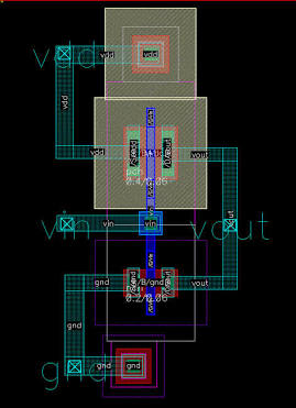
Enables coupling-capacitance requirements to be addressed before physical layout through automated spacing guidance, potentially reducing design iterations, development time and layout-related errors.
IC designers need to manage coupling capacitance between metal layers, but determining appropriate spacing can be complex and may require late-stage or iterative layout adjustments, potentially increasing design time and affecting circuit performance.
Provides an automated IC-layout planning method that obtains process-design-kit spacing rules, maps coupling-capacitance values to corresponding metal-layer spacing and determines appropriate spacing requirements before physical layout begins.
Introduces a pre-layout method for translating coupling-capacitance requirements into metal-layer spacing using PDK rules and a lookup table, enabling designers to address capacitance constraints before physical layout begins.